On August 4, 2026, at the Future of Memory and Storage (FMS 2026) conference held in Santa Clara, California, Samsung Electronics formally unveiled the industry’s first zHBM concept model, alongside a vertical stacking solution for NAND flash named zNAND‑O. Designed for next‑generation ultra‑scale AI computing, zHBM represents a groundbreaking memory architecture that vertically integrates high‑bandwidth memory (HBM) directly atop an AI accelerator die. This marks a significant departure from conventional 2.5D packaging, and is widely seen as a key technological path to overcoming the “memory wall” bottleneck that hampers AI performance scaling.
Architectural Revolution: From Side‑by‑Side to True 3D Vertical Stacking
The “z” in zHBM denotes the vertical Z‑axis in three‑dimensional space. The core innovation lies in fundamentally re‑architecting the integration of HBM with compute logic: moving away from the long‑established 2.5D side‑by‑side layout to a true 3D vertical fusion.
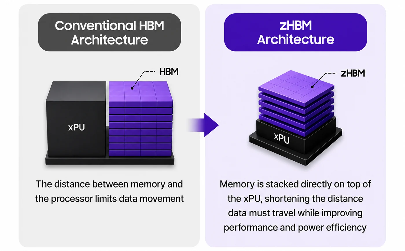
In conventional HBM implementations, the HBM stacks and the AI accelerator chip are placed side‑by‑side on the same package substrate, interconnected via a silicon interposer. Data travels across relatively long horizontal traces on the interposer, which imposes physical limits on latency, power consumption, and package footprint. This arrangement struggles to keep pace with the exponential growth in AI compute and its ever‑increasing memory bandwidth requirements.
zHBM eliminates the horizontal transmission path entirely by stacking the entire HBM memory directly above the AI accelerator die. This reduction in data travel distance approaches the physical limit, fundamentally lowering latency and interconnect power, while dramatically saving substrate real estate. As a result, both compute density and memory density per unit area are significantly enhanced, achieving a deep, three‑dimensional integration of computation and memory.
Key Performance Metrics
Using Samsung’s yet‑to‑be‑mass‑produced next‑generation HBM5 as a baseline, the company disclosed anticipated performance figures for the zHBM concept. The table below highlights the key differences:
| Performance Dimension | HBM5 | zHBM Concept |
|---|---|---|
| Overall Performance | Baseline | 4× – 8× that of HBM5 |
| Memory Density | Baseline | >10× that of HBM5 |
| Power Efficiency | Baseline | 3× improvement |
| Overall Thermal Resistance | Baseline | >50% reduction |
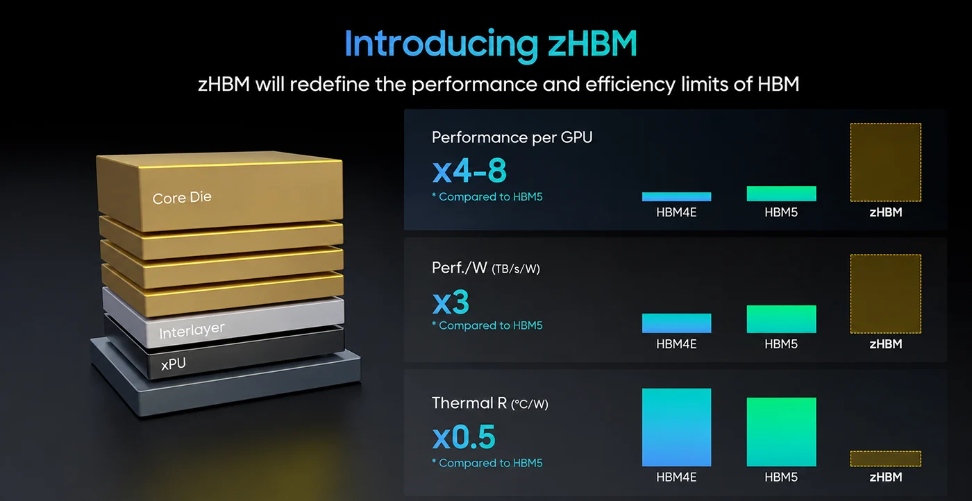
These gains are not only driven by the shorter transmission path but also by an all‑new memory interface system. Additionally, zHBM supports customer‑specific customization by allowing dedicated IP blocks to be embedded in the interlayer between the memory stack and the AI accelerator, enabling flexible memory capacity expansion or tailored accelerator logic to suit the unique requirements of different AI chip vendors.
Three Core Enabling Technologies
Realizing the zHBM architecture depends on a combination of advanced semiconductor process innovations. Three key technologies form the foundation of this solution:
Wafer‑Level Hybrid Copper Bonding. This is the fundamental process for achieving high‑density vertical stacking. Replacing traditional micro‑bump connections, it employs direct copper‑to‑copper bonding for chip‑to‑chip interconnects, boosting interconnect density by an order of magnitude while significantly reducing contact resistance and signal loss. This enables taller memory stacks and higher data rates, making 3D integration viable from a manufacturing standpoint.
Multi‑Wafer Stacking Integration. Leveraging know‑how from V‑NAND vertical stacking and through‑silicon via (TSV) technology, zHBM integrates multiple DRAM wafers with the compute wafer into a single monolithic 3D structure. This technology underpins the tenfold increase in memory density, while also ensuring robust electrical stability across the stack.
Targeted Thermal Management Optimization. To address the concentrated heat dissipation challenge inherent in vertical stacking, Samsung has reduced overall thermal resistance through careful material selection and structural design. In addition, the high‑thermal‑conductivity pathways from wafer bonding serve as auxiliary heat‑spreading channels, alleviating thermal accumulation above the power‑hungry compute die, thereby ensuring long‑term reliability for high‑capacity stacking.
Roadmap and Technology Positioning
At present, zHBM remains a proof‑of‑concept. Samsung has not announced a specific mass‑production timeline. Industry consensus places commercialization roughly in the 2028–2029 timeframe. On Samsung’s current memory roadmap, near‑term production efforts are focused on HBM4, which entered mass production in February 2026. In May 2026, the company began delivering HBM4E samples, and the second half of 2026 is dedicated to expanding HBM4 capacity. Both HBM5 and zHBM are positioned as longer‑term developments, to be phased in as AI compute demands and manufacturing maturity evolve.
Unlike HBF (High‑Bandwidth Flash), which is a NAND‑based flash stacking solution designed for high capacity and low cost primarily for storing AI model weights, zHBM is a DRAM‑based high‑bandwidth memory that emphasizes ultra‑low latency and extremely high bandwidth, tailored for real‑time AI inference and training. Moreover, zHBM differs from conventional HBM internal stacking. While regular HBM stacks only DRAM dies within the memory module and remains placed side‑by‑side with the compute chip, zHBM achieves cross‑category vertical integration of the entire memory subsystem with the compute chip, offering a much higher level of integration.
Commercialization Challenges
As a forward‑looking technology, zHBM faces multiple engineering hurdles before large‑scale deployment.
- Yield is a major concern: wafer‑level bonding demands sub‑micron alignment accuracy, and multi‑layer stacking tends to cause yield to drop exponentially. This imposes stringent requirements on front‑end cleanliness and equipment precision, keeping near‑term manufacturing costs high.
- Thermal performance remains to be fully validated in practical systems: despite the claimed thermal resistance improvement, the memory sits directly above a heat‑generating compute die, leading to significant localized heat concentration. The actual effectiveness of the cooling solution under heavy workloads still requires extensive engineering verification.
- The architecture forces AI chip designers to re‑think their chip floorplans, packaging, and memory controllers—a long and costly co‑development cycle involving the entire supply chain.
zHBM represents an important technological exploration in the post‑Moore era, aiming for deeper integration of memory and computing. It breaks through the bandwidth ceiling of traditional 2.5D packaging and provides a stronger memory foundation for next‑generation ultra‑scale AI training and large language model inference. More broadly, it signals a shift in high‑end HBM evolution—from intra‑memory stacking toward true compute‑memory vertical integration—and will likely drive further advances in advanced packaging and memory technologies, laying the groundwork for sustained AI performance scaling.