As AI models grow, high bandwidth memory (HBM) is built with more layers and higher speeds to keep up. However, this increases heat, especially in the die‑to‑die physical layer (D2D PHY), the interface that handles ultra‑fast data transfer between HBM and the AI chip. This small area becomes the hottest spot on the chip. Traditional HBM forces heat to travel through several core die layers before it can escape, which is a long and inefficient path. If heat is not removed quickly, the chip temperature rises and triggers throttling — a self‑protection mechanism that lowers performance. Solving this heat bottleneck is essential to unlock the full power of next‑generation AI chips.
Core Component and How iHBM Works
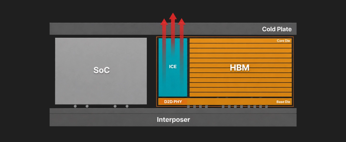
SK Hynix has proposed a solution to this heat problem called integrated high bandwidth memory, or iHBM. The core of this technology is a special cooling component embedded inside the HBM. This component is named ICE. ICE is made of a silicon‑based material. This material has two key properties at the same time. First, it has high thermal conductivity, meaning it transfers heat efficiently. Second, it is electrically insulating, so it can be placed safely among dense circuits without causing short circuits. The ICE component is placed directly in the D2D PHY area, where heat is most concentrated and data exchange between HBM and the processor is the heaviest.
In traditional HBM design, heat must pass through multiple core die layers before leaving the chip. That path is long. iHBM changes this path. By using the embedded ICE component, it creates a dedicated heat channel inside the chip. Heat can now travel almost directly from the source to the package case or heat spreader, without going through many functional layers. This shortens the heat path and lowers the resistance that heat meets along the way.
From a manufacturing perspective, iHBM is built on SK Hynix‘s already mass‑produced MR‑MUF wafer‑level packaging technology. MR‑MUF stands for mass reflow molded underfill, a process that delivers high production efficiency and good yield. Adding the ICE component embedding step to this existing process makes mass production of iHBM feasible.
Key Advantages Of iHBM
The iHBM technology delivers several clear benefits by changing the heat path.
- Better cooling. According to data released by SK Hynix, iHBM reduces thermal resistance by more than 30% compared to traditional HBM cooling solutions. Thermal resistance is a measure of how hard it is for heat to flow. Lower thermal resistance means heat generated inside the chip is removed more easily. For a high‑power density area like the D2D PHY, a 30% reduction in thermal resistance can significantly lower operating temperature.
- Improved system stability. Once temperature is well controlled, system stability improves. During long, heavy workloads such as AI training and inference, high chip temperature can trigger throttling, which reduces computing power. With the iHBM solution, the chip can stay at its peak performance for longer periods and suffer fewer throttling events. This is especially important for large model training tasks that need to run continuously for days or even weeks.
- Low deployment barrier. Another advantage of iHBM is ease of deployment. The technology maintains high design compatibility with existing system‑in‑package environments. This means that HBM modules using iHBM can replace traditional HBM modules without major redesign of the GPU or AI accelerator package. For chip makers and cloud service providers, this reduces the time and cost needed for technology validation and product integration.
- Ready for mass production. On manufacturability, iHBM is based on SK Hynix’s mature MR‑MUF wafer‑level packaging process. This process has been proven over multiple generations of HBM products, with high yield and volume production capability. Adding the ICE component embedding step to an existing production line does not require rebuilding the entire manufacturing flow. This gives iHBM a clear path from lab to large‑scale commercial use.
Main Use Cases
The iHBM technology solves the problem of heat management in high‑power density areas, so its main use cases are in fields that demand both high computing power and high energy consumption.
High‑performance computing(HPC). HPC often involves complex scientific simulations, weather forecasting, genome analysis, and similar tasks. These tasks require many computing nodes to work in parallel, and they often run for hours or even days. In such environments, chips stay under heavy load for long periods, and heat builds up continuously. If cooling is insufficient, computing clusters will slow down due to temperature protection, extending total computation time. iHBM helps chips maintain a stable temperature by lowering thermal resistance, thereby ensuring sustained computing power.
AI data centers. As generative AI and large language models spread, the power density of AI data centers is rising fast. A single AI server can already consume several kilowatts, with HBM and GPU being the main heat sources. Data centers not only need to cool the chips but also must consider the energy and space costs of the entire cooling system. More efficient chip‑level cooling means less reliance on liquid cooling or high‑speed fans, reducing both capital investment and operating expenses for cooling equipment. iHBM manages heat directly inside the chip, helping to reduce the burden of heat removal from the source.
Future edge AI devices. Currently the most urgent cooling needs are in data centers. But as AI capabilities move into phones, personal computers, cars, and other end devices, the cooling challenges in these compact spaces will grow. End devices have limited space for cooling and cannot fit large fans or liquid cooling systems, so they depend more on the chip‘s own cooling efficiency. Although iHBM is currently aimed at enterprise‑grade memory products like HBM5, the same idea — embedding a dedicated cooling component in the hot spot — could inspire cooling designs for mobile devices.
Beyond these, any system that uses high bandwidth memory and faces cooling bottlenecks could benefit from iHBM technology. For example, high‑performance computing platforms for autonomous driving and edge computing servers need to control temperature under high‑density deployment. As computing demand keeps growing, heat management is shifting from a secondary system issue to a core problem that determines performance limits. The direction that iHBM represents therefore has broader significance.
Competitive Landscape of Cooling Technologies
As the power density of HBM continues to rise, cooling capability is becoming a key factor that determines the competitiveness of next‑generation HBM products. The three major memory makers — SK Hynix, Samsung Electronics, and Micron Technology — as well as some cloud service providers are all exploring different cooling technology paths.
| Company | Technology | Core Idea | Key Data |
|---|---|---|---|
| SK Hynix | iHBM | Embed a high‑thermal‑conductivity, electrically insulating cooling component inside the HBM‘s hot D2D PHY area, creating a dedicated heat path | >30% reduction in thermal resistance |
| Samsung Electronics | HPB cooling + hybrid copper bonding | Change chip stacking structure by moving DRAM to the side of the processor and placing a copper heat spreader directly above the processor core; use copper‑to‑copper bonding to eliminate thermal resistance | ~30% temperature reduction; 16% improvement in thermal impedance |
| Micron Technology | Circuit design improvement + enhanced base die | Improve cooling while boosting performance by refining internal circuit design and optimizing base die performance | >20% improvement in energy efficiency |
| Microsoft | Microfluidic cooling | Etch micro‑channels on the back of the silicon chip and deliver coolant directly to the heat sources inside the chip | 2‑3x better heat removal than cold plates; 65% reduction in peak temperature rise |
In summary, SK Hynix has built an early lead in cooling with iHBM technology. Samsung is catching up quickly with its HPB and hybrid copper bonding approaches. Micron remains competitive through steady process improvements in energy efficiency. At the same time, cloud service providers like Microsoft are exploring microfluidic cooling from the system level, opening new possibilities for cooling even higher‑power AI chips in the future.
Conclusion and Outlook
SK Hynix‘s iHBM technology addresses a long‑ignored but increasingly urgent problem: how to efficiently remove heat from hot spots inside high bandwidth memory. For AI data center and high‑performance computing users, better cooling means more stable computing power, lower cooling energy costs, and longer equipment life. As AI models continue to grow in size, HBM stack layers and power density will rise further. It is likely that heat management will shift from a secondary issue in system design to a core problem that determines the feasibility of next‑generation AI infrastructure. The direction that iHBM represents — solving heat problems at the source, inside the package — offers a practical path forward for this challenge.