As DDR5 memory has just completed its initial penetration in the consumer market and continues to steadily increase its adoption in the server sector, discussions about DDR6 have quietly started to heat up both inside and outside the industry. This is not an “overly premature hype” in the technology field, but an inevitable result of market demand and technological evolution. At present, fields such as generative artificial intelligence, high-performance computing, and cloud computing are experiencing explosive growth, placing unprecedentedly strict requirements on memory bandwidth, capacity, and energy efficiency. According to forecasts by TrendForce, from 2024 to 2026, AI- and server-related applications will account for 46%, 56%, and 66% of total DRAM capacity demand respectively, and this figure is expected to exceed 70% in 2027. Even the current most powerful DDR5 memory is gradually becoming insufficient to meet the massive data throughput requirements of AI training and large-scale data processing scenarios.
At the same time, in the consumer market, high-end gaming laptops and mobile workstations continue to pursue higher memory frequencies and larger capacities, while thin-and-light devices impose strict limitations on memory power consumption and physical space. All of these factors are accelerating the development of a new generation of memory standards. Major global memory manufacturers such as Samsung, SK hynix, and Micron have already completed early prototype development of DDR6 specifications and are working together with chip vendors including Intel, AMD, and NVIDIA to advance platform validation.
How DDR Memory Has Evolved
What Is DDR Memory, and Why Is “Bandwidth” So Important
DDR memory, short for Double Data Rate Synchronous Dynamic Random Access Memory, is the core component in computer systems responsible for temporarily storing data. It also serves as the data transfer bridge between the CPU and storage devices such as hard drives. Its core working principle is based on a synchronous clock signal that allows data to be transferred on both the rising and falling edges of each clock cycle. As a result, data transfer efficiency is doubled at the same clock frequency, which is where the term “double data rate” comes from.
Among all performance metrics of DDR memory, bandwidth is undoubtedly the most critical. Memory bandwidth refers to the amount of data that memory can transfer per unit of time. It is calculated using the formula: bandwidth = memory frequency × bus width × number of channels ÷ 8. Bandwidth directly determines how fast the CPU can access data. It can be compared to a “highway” for data transmission: the wider the highway, the higher the data transfer efficiency. In complex application scenarios, such as running large AAA games, performing video editing and rendering, or training AI models, the CPU needs to continuously read and write large amounts of data at high speed. If memory bandwidth is insufficient, “data congestion” occurs, causing the CPU to wait for data for extended periods. In such cases, even a very powerful CPU cannot fully perform, creating a system performance bottleneck. Therefore, improving memory bandwidth has always been one of the core goals in the evolution of each generation of DDR memory technology.
From DDR1 to DDR5: What Problems Each Generation Solved
From DDR1 to DDR5, each generation of memory was designed to directly address the key challenges faced by the industry at the time, achieving significant performance improvements through technological innovation. DDR1, the first generation of DDR memory, emerged around the year 2000. Its core breakthrough was the implementation of double data rate transmission, replacing traditional SDRAM and initially solving the problem of insufficient memory transfer speeds in early computer systems. It provided compatible memory support for early processors such as the Pentium 4, with data rates ranging from 200 to 400 MT/s.
DDR2 memory was introduced around 2004 and primarily addressed the limitations of DDR1, including its low maximum speed and relatively high power consumption. By improving memory chip manufacturing processes and signal processing technologies, DDR2 increased data rates to 533–800 MT/s, while reducing operating voltage from 2.5 V in DDR1 to 1.8 V. This significantly lowered power consumption and heat generation, making it better suited to the development of multi-core processors at the time.
DDR3 memory, which appeared in 2007, further broke through speed limitations, raising the maximum data rate to 1600 MT/s and reducing operating voltage to 1.5 V, resulting in a major improvement in energy efficiency. More importantly, DDR3 improved memory stability and compatibility through optimized memory controller design. It supported widespread adoption across laptops, desktops, and servers, becoming one of the longest-lasting memory standards.
DDR4 memory, launched in 2014, was designed to meet the dual demands for memory capacity and bandwidth in the era of big data. It increased data rates to 2133–3200 MT/s and reduced operating voltage to 1.2 V, while also supporting much larger single-module capacities, with a maximum of up to 128 GB per module. By introducing Bank Group technology, DDR4 improved concurrent memory access capabilities and effectively reduced bandwidth pressure in multitasking scenarios, becoming the mainstream memory configuration for computer systems over the past decade.
DDR5 memory, officially commercialized at the end of 2021, achieved another major leap in speed and energy efficiency to meet early AI and high-performance computing requirements. Its maximum data rate reaches up to 8000 MT/s, operating voltage is further reduced to 1.1 V, and it adopts a 2 × 32-bit channel structure to enhance parallel processing capabilities. DDR5 also introduced on-die ECC error correction for the first time in consumer memory, improving data transmission stability, with single-module capacities reaching up to 256 GB. However, as AI applications continue to grow explosively, the performance limits of DDR5 are gradually becoming apparent, laying the groundwork for the development of DDR6.
What Is DDR6
DDR6 is the next-generation Double Data Rate Synchronous Dynamic Random Access Memory standard led by JEDEC (the Joint Electron Device Engineering Council). It is designed to address the extreme demands for memory bandwidth, capacity, and energy efficiency driven by emerging fields such as artificial intelligence, high-performance computing, and cloud computing. The DDR6 standardization process officially began in 2024, with the core objective of breaking through the physical performance limits of DDR5 and creating a memory platform that offers high bandwidth, large capacity, high energy efficiency, and high reliability.
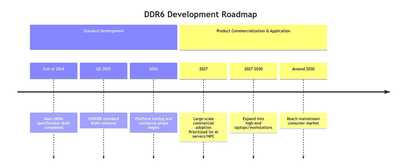
By the end of 2024, JEDEC completed the main draft specification of DDR6, laying the foundation for subsequent technology development and product implementation. At the same time, the draft specification for the low-power version, LPDDR6, was released in the second quarter of 2025. Similar to previous memory standard development processes, the formulation of DDR6 brings together major global memory manufacturers, chip designers, and end-device vendors. This ensures that the standard can support different application scenarios and hardware platforms, while promoting coordinated development across the entire industry ecosystem.
The Three Core Problems DDR6 Aims to Solve
The development of DDR6 focuses on addressing three core challenges currently faced by the industry: insufficient bandwidth, low energy efficiency, and architectural limitations.
The first issue is insufficient bandwidth. With rapidly growing demand from AI training and large-scale data processing, the current maximum speed of DDR5 at 8000 MT/s is increasingly unable to meet the requirements for high-speed transmission of massive amounts of data, becoming a key bottleneck limiting overall system performance. DDR6 improves channel architecture and transmission technologies to raise the initial data rate to 8800 MT/s, with plans to increase it to 17,600 MT/s in later stages, aiming to fundamentally eliminate bandwidth bottlenecks in high-load scenarios.
The second issue is energy efficiency. In AI servers and data center environments, memory modules are deployed at increasingly high densities, which significantly increases power consumption and heat generation. This not only raises operating costs but also places greater demands on cooling systems. By reducing operating voltage and optimizing power management mechanisms, DDR6 improves performance while lowering power consumption. Typical power consumption is expected to be reduced by 15–20% compared with DDR5, making DDR6 better suited for high-density deployment scenarios.
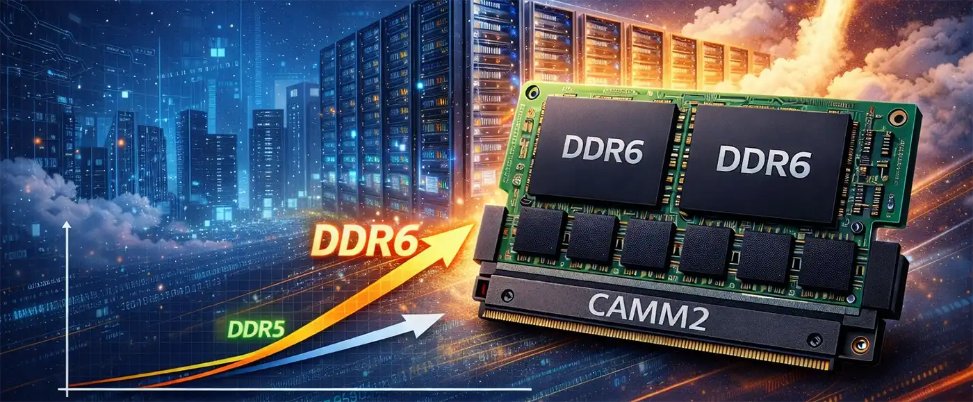
The third issue is architectural limitations. The 2 × 32-bit channel structure used by DDR5 is prone to signal integrity issues at high frequencies. In addition, traditional DIMM and SO-DIMM form factors suffer from large space requirements and frequency limitations under 2DPC configurations. DDR6 introduces an innovative 4 × 24-bit sub-channel architecture and adopts the CAMM2 interface standard. This not only improves parallel processing capability but also addresses space and frequency constraints of traditional memory packaging, providing architectural support for high-performance and high-density memory deployment.
Key Technical Changes in DDR6
A Major Leap in Data Transfer Speed
A significant increase in data transfer speed is one of the most important technological breakthroughs of DDR6. According to current industry roadmaps, DDR6 will start with an initial data rate of 8800 MT/s, already exceeding the current maximum of DDR5 at 8000 MT/s. Over its entire product lifecycle, DDR6 speeds are expected to increase further to 17,600 MT/s, with some overclocked versions potentially exceeding 21,000 MT/s. Overall performance is expected to be approximately two to three times higher than DDR5.
Such a substantial speed increase is not achieved simply by raising clock frequency. Instead, it results from the combined effect of multiple technologies. On one hand, DDR6 optimizes memory chip manufacturing processes, improving electrical performance and providing a hardware foundation for high-frequency operation. On the other hand, DDR6 introduces more advanced signal integrity optimization designs, including improved packaging technologies, finer routing rules, and stricter timing control. These measures effectively reduce signal interference and attenuation at high frequencies. In addition, DDR6 adopts a 16n prefetch mechanism, compared with the 8n prefetch used in DDR5. This further improves data transfer efficiency, allowing more data to be transmitted at the same clock frequency and enabling a major leap in overall transfer speed.
Changes in Sub-Channel Architecture
DDR6 introduces a disruptive innovation in channel architecture by adopting a 4 × 24-bit sub-channel structure, replacing the 2 × 32-bit channel design used by DDR5. The core goal of this architectural change is to improve bandwidth while maintaining signal integrity at high operating frequencies. Traditional wide bus designs tend to suffer from signal crosstalk when frequencies increase beyond a certain point, leading to reduced transmission stability. By increasing the number of channels and reducing the bit width of each channel, DDR6 expands the total bus width from 64 bits in DDR5 to 96 bits. This approach enhances parallel processing capability while reducing signal transmission pressure on each individual channel.
The 4 × 24-bit sub-channel architecture enables more efficient parallel data transmission, allowing each sub-channel to independently perform read and write operations. This significantly improves memory concurrency and bandwidth utilization. In scenarios such as AI training and large-scale data processing, where multiple data streams must be handled simultaneously, the advantages of this architecture become especially apparent. At the same time, the sub-channel architecture provides greater flexibility for capacity expansion and energy efficiency optimization. It allows the operating state of each sub-channel to be dynamically adjusted according to application requirements, achieving a better balance between performance and power consumption.
Changes in Module and Interface Form Factors (CAMM2)
DDR6 will fully adopt the CAMM2 interface standard, replacing the traditional DIMM and SO-DIMM interfaces that have been used for many years. This represents a major transformation in memory module form factors. CAMM2 stands for Compression Attached Memory Module. It was originally introduced by Dell, later revised by JEDEC, and officially became a JEDEC standard at the end of 2023. Unlike traditional memory modules that connect to slots via edge connectors at the bottom, CAMM2 uses a compression connector that connects through a thin adapter board on the motherboard and is secured with screws. This new interface form brings several significant advantages:
CAMM2 effectively resolves the frequency limitations found in traditional 2DPC configurations. In conventional 2DPC designs, installing two memory modules per channel increases electrical complexity and limits memory frequency. CAMM2 moves the complex topology into the module itself, handling complexity internally and allowing a system to achieve both maximum performance and maximum capacity at the same time.
CAMM2 significantly reduces Z-axis height and overall motherboard space usage. Compared with SO-DIMM, CAMM2 reduces thickness by 57%, making it more suitable for devices with strict thickness requirements, such as thin-and-light laptops and tablet computers.
The CAMM2 connector uses an LGA pin design, with contact pads on both the motherboard and the memory module. This reduces the risk of interface damage, and the connector itself can be replaced independently, making maintenance more convenient.
Further Evolution of Energy Efficiency and Power Management
In terms of energy efficiency optimization, DDR6 builds on the low-power advantages of DDR5 and achieves further breakthroughs. The standard operating voltage of DDR5 is 1.1 V, while DDR6 will reduce operating voltage to 1.0 V or even lower. Lower voltage directly leads to reduced power consumption, with typical DDR6 power consumption expected to be 15–20% lower than DDR5. This improvement is especially critical for high-density deployment scenarios such as data centers and AI servers, as it helps reduce overall energy consumption and cooling costs while improving system energy efficiency.
In addition to lowering operating voltage, DDR6 introduces more advanced power management mechanisms. By optimizing the power management logic of the memory controller, DDR6 can dynamically adjust the operating state of memory modules based on system load. Under low-load conditions, memory frequency and voltage are automatically reduced, allowing the system to enter low-power modes. Under high-load conditions, performance is rapidly increased to ensure data transmission requirements are met. This dynamic power management approach allows DDR6 to achieve an optimal balance between performance and power consumption across different application scenarios, delivering high performance while effectively conserving energy.
Capacity Expansion and Stacking Potential
DDR6 offers greater potential for capacity expansion, making it better suited to meet the large memory capacity requirements of AI and high-performance computing workloads. Innovations in stacking technology are a key enabler of DDR6 capacity scaling. DDR6 will adopt more advanced 3D stacking packaging technologies, stacking more memory dies vertically to significantly increase capacity density per chip. At the same time, the modular design of the CAMM2 interface facilitates capacity expansion by supporting stacked module configurations to increase total system memory capacity.
For example, two single-channel D-type CAMM2 modules can theoretically be stacked along the Z-axis, allowing total system memory to reach 512 GB. As the technology matures, even higher capacity breakthroughs may be achieved. Currently planned DDR5 CAMM2 modules can reach a maximum capacity of 256 GB. With higher-density memory chips and stacking technologies, DDR6 CAMM2 modules are expected to surpass this limit.
A Comprehensive Comparison Between DDR6 and DDR5
| Category | DDR5 | DDR6 |
|---|---|---|
| Data Rate | Up to about 8000 MT/s | Initial 8800 MT/s, planned to increase to 17,600 MT/s, overclocked versions may exceed 21,000 MT/s |
| Channel Architecture | 2 × 32-bit (total bus width 64-bit) | 4 × 24-bit (total bus width 96-bit) |
| Interface Form Factor | Mainly DIMM, SO-DIMM | Fully adopts CAMM2 / LPCAMM2 |
| Operating Voltage | 1.1 V | 1.0 V or lower |
| Typical Power Consumption | Baseline level | 15–20% lower than DDR5 |
| Maximum Capacity per Module | 256 GB (DIMM), 128 GB (SO-DIMM) | Expected to exceed 256 GB, dual-module stacking may achieve 512 GB |
| Prefetch Mechanism | 8n prefetch | 16n prefetch |
| 2DPC Frequency Limitation | Significant frequency limitations | Complexity handled within the module, no obvious frequency limitation |
| Main Application Scenarios | Mid- to high-end PCs, servers, workstations (transition period) | AI servers, high-performance computing, high-end workstations, flagship PCs |
Compatibility of DDR6
There is no backward compatibility between DDR6 and DDR5. This means that motherboards designed for DDR5 cannot directly use DDR6 memory, and vice versa. The core reason lies in fundamental differences in architecture, interface form factors, and electrical specifications.
First, there is a difference in interface form factor. DDR6 fully adopts the CAMM2 interface, while DDR5 mainly uses traditional DIMM and SO-DIMM interfaces. Their physical dimensions and connection methods are completely different, making them incompatible with each other.
Second, there are differences in electrical specifications. DDR6 reduces operating voltage to 1.0 V or even lower, compared with 1.1 V for DDR5. In addition, their signal definitions and timing parameters are entirely different. Memory controllers must be designed with specific electrical specifications in mind to drive circuits and handle signals correctly. A DDR5 memory controller cannot meet the electrical requirements of DDR6, and forced use would result in device damage or failure to operate properly.
Finally, there are differences in channel architecture. DDR6 uses a 4 × 24-bit sub-channel architecture, which is fundamentally different from the 2 × 32-bit architecture used by DDR5. The design logic of the memory controller is completely different in each case, which ultimately determines that the two standards are incompatible. Therefore, the deployment of DDR6 requires coordinated support from CPUs, motherboards, and the entire industry ecosystem to form a complete hardware support system. At present, memory manufacturers such as Samsung, SK hynix, and Micron are working closely with chip vendors including Intel, AMD, and NVIDIA to jointly advance DDR6 platform validation and accelerate ecosystem development.
Application Scenario Analysis of DDR6
Data Centers and Cloud Computing
Data centers and cloud computing are among the most important application scenarios for DDR6. Currently, cloud computing services are evolving toward large scale, high concurrency, and low latency. Data centers must handle massive numbers of user requests and data transfer tasks, placing extremely high demands on memory bandwidth and capacity. DDR6 can significantly increase memory bandwidth in data center servers, speeding up data processing and transmission while reducing response latency for user requests.
At the same time, the high energy efficiency of DDR6 is well suited to data center requirements. Data centers operate with high server density, and memory modules account for a substantial portion of total system power consumption. Compared with DDR5, DDR6 reduces power consumption by 15–20%, which can effectively lower overall energy usage and cooling costs in data centers while improving operational efficiency. In addition, DDR6 supports large-capacity expansion, meeting the needs of large-scale data caching and parallel processing in cloud computing environments. This provides stronger memory support for services such as cloud databases, cloud storage, and cloud rendering. With the commercial adoption of DDR6, data center computing and data processing capabilities are expected to achieve a qualitative leap.
AI and High-Performance Computing (HPC)
AI and high-performance computing are the core driving forces behind the development and adoption of DDR6, and they are also the application scenarios where DDR6 can deliver the greatest advantages. In AI training scenarios, model parameter sizes continue to grow, requiring the processing of massive amounts of training data. This places extreme demands on memory bandwidth and capacity. The high-bandwidth characteristics of DDR6 ensure that CPUs and GPUs can quickly read and write training data during the training process, avoiding data transfer bottlenecks and significantly improving training efficiency.
In the field of high-performance computing, such as weather forecasting, astrophysics simulations, and pharmaceutical research, systems must perform large volumes of complex calculations and data processing. These workloads require extremely high levels of parallel processing capability and stability from memory. The 4 × 24-bit sub-channel architecture of DDR6 enhances parallel data processing, while the 16n prefetch mechanism and advanced error correction mechanisms ensure both efficiency and stability in data transmission. In addition, the low-power advantages of DDR6 help reduce energy consumption in high-performance computing clusters, improving their ability to operate continuously over long periods. As AI and high-performance computing continue to expand, DDR6 will become a core memory configuration in these fields.
Consumer PCs and High-End Workstations
Although DDR6 will be commercially deployed first in servers and AI-related fields, it is expected to gradually penetrate the consumer PC and high-end workstation markets as the ecosystem matures and costs decline. For high-end gaming laptops and flagship desktop PCs, the high frequency and high bandwidth of DDR6 can improve game loading times and overall smoothness. This is especially noticeable when running large AAA games, where DDR6 can effectively reduce stuttering and frame drops. At the same time, the thin design enabled by the CAMM2 interface helps manufacturers create thinner and lighter gaming laptops with high performance.
High-end workstations will also be among the first consumer segments to adopt DDR6. Mobile workstations and graphics workstations are primarily used for professional workloads such as video editing, 3D modeling, and animation rendering, which place very high demands on memory frequency, capacity, and stability. Traditional SO-DIMM memory suffers from frequency limitations under 2DPC configurations and cannot meet the performance requirements of high-end workstations. DDR6 combined with the CAMM2 interface addresses this issue while also providing greater capacity support.
Standardization Progress and Commercialization Timeline
The organization responsible for leading memory technology standards, JEDEC, completed the draft of the main DDR6 specification at the end of 2024. The draft standard for LPDDR6, targeting mobile devices, was also released in the second quarter of 2025. The next stage will be the critical platform testing and validation phase, which is expected to take place in 2026. Chip manufacturers such as Intel and AMD will participate to ensure compatibility between DDR6 and future processor platforms.
According to industry forecasts, DDR6 is expected to enter large-scale commercial deployment around 2027. Its adoption path is expected to follow a high-end-to-mainstream pattern. It will first be used in fields that are extremely sensitive to performance but less sensitive to cost, such as AI servers, high-performance computing systems, and data centers. It will then gradually expand into high-end laptops and workstation markets. Mainstream desktop PCs and ordinary laptop users may not widely encounter DDR6 until around 2030.
DDR6 is not a simple iteration, but an architectural evolution designed to address fundamental challenges. Its core goal is to break through current bottlenecks in memory bandwidth and energy efficiency, providing essential infrastructure support for artificial intelligence, high-performance computing, and future large-scale data processing. The journey from DDR1 to DDR5 demonstrates a consistent pattern in which memory technology continuously evolves to match computing demands. DDR6 represents the next chapter in this progression. It carries the mission of expanding the boundaries of computing, and its final form and widespread adoption will have a profound impact on the trajectory of technological development over the next decade.


